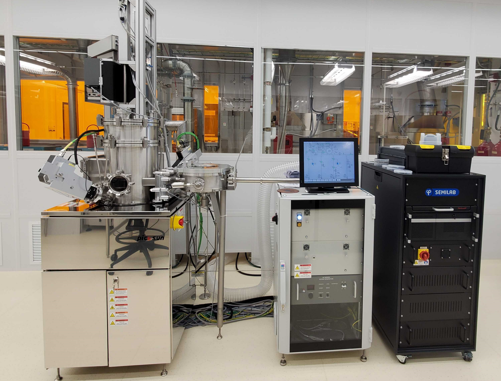
Overview
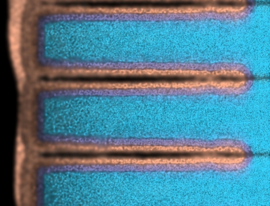
The PicoSun R-200 Advanced system facilitates Plasma-Enhanced Atomic Layer Deposition (PE-ALD), a vapor deposition method which uses sequential, self-limiting surface reactions to deposit thin films submonolayers at a time. This provides precise thickness control and highly conformal thin films for ultrathin film applications, high aspect ratio features and porous materials.
Capabilities
- Precursors: TMA (Trimethylaluminum), TiCl4, TDMATi [Tetrakis(dimethylamido) titanium], H2O, O3, NH3
- Deposited films: Al2O3, AlN, TiO2, TiN
- Deposition rates: ~0.2 - 1.2 Å/cycle, depending on process
- Substrate Temperature: 50℃ - 500℃, plasma 450℃
- Sample types:
- Wafers - up to 200 mm diameter (8 inch)
- 156 mm x 156 mm solar Si wafers
- 3D samples
- Porous materials
- Powders and particles
Contact
-

VINSE Cleanroom
Dr. Ben Schmidt, Manager
Dr. Christina McGahan
Megan Dernberger- 111 Engineering Science Building