 Jacob “Jake” Grayson
Graduate Student, Physics & Astronomy
Richard Haglund Research Group
My research focuses on harnessing optical phase-change materials to enable new forms of active control in nanophotonic devices. In particular, I have been working to integrate vanadium dioxide (VO₂)—a material that undergoes a dramatic, reversible metal–insulator transition—into valley photonic crystals to realize actively reconfigurable topological photonic circuits. By embedding VO₂ into carefully engineered photonic crystal geometries, I aim to create on-chip optical routing devices that can dynamically switch between distinct topological states, allowing robust light transport that can be turned “on” and “off” with optical or thermal stimuli.
This approach draws inspiration from the field of valley photonics, where distinct valleys in the photonic band structure can be selectively addressed to guide light along protected pathways. The addition of a phase-change material offers an unprecedented degree of reconfigurability, potentially enabling compact, energy-efficient, and fault-tolerant routing elements for photonic integrated circuits. My work combines computational design of photonic band structures with fabrication of dual-material photonic crystal lattices and will ultimately integrate ultrafast pump–probe experiments to directly observe the switching dynamics in these hybrid systems.
In parallel, I am exploring whether nanostructured metasurfaces composed of phase-change vanadates—specifically VO₂ and vanadium sesquioxide (V₂O₃)—can lower the energy threshold for triggering their phase transitions through resonant optical field confinement. By patterning these correlated electron materials into dielectric resonators and metasurface arrays, it may be possible to concentrate incident light within the active material volume, enhancing the local optical intensity and reducing the input power needed for switching. This work combines electromagnetic simulations, nanofabrication, and ultrafast optical characterization to directly probe switching thresholds and identify geometries that maximize field enhancement.
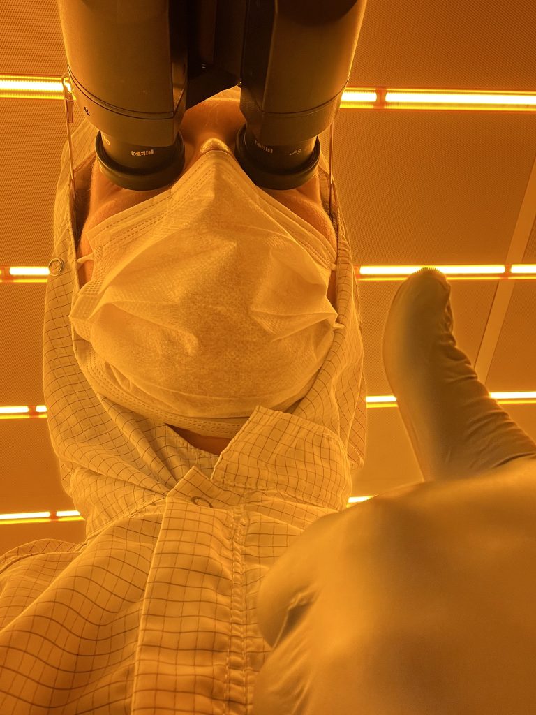 These threads of investigation have required the development of nanofabrication workflows that integrate high-precision electron beam lithography, thin-film material deposition, dry etching, and advanced imaging techniques while maintaining the structural and stoichiometric integrity of VO₂ and V₂O₃ at the nanoscale. My journey at Vanderbilt has been defined by moving fluidly between computational design, cleanroom fabrication, and tailored optical spectroscopy, with each stage informing the next. From simulating topological band structures to patterning subwavelength resonators and capturing femtosecond-scale switching events, my work seeks to bridge fundamental photonic physics with practical, reconfigurable device architectures.
Looking ahead, two exciting new opportunities will take my research off campus. Soon, I will go to Oak Ridge National Laboratory to fabricate these types of phase-change photonic metamaterials at the Center for Nanophase Material Science (CNMS) as part of an approved user proposal. Later this year, I will travel to the Institute for Photonic Sciences (ICFO) in Barcelona, Spain to work with the Attoscience and Ultrafast Optics Group, where we’ll carry out high-resolution, time-resolved spectroscopies to probe the ultrafast dynamics and symmetry-breaking phenomena in these nanoengineered materials.
My VINSE Story
Working within VINSE has been the foundation of my growth as a researcher. The breadth of tools, facilities, and expertise available under one roof has given me the freedom to explore ambitious ideas, even when some paths didn’t lead where I expected. That flexibility has allowed me to pivot seamlessly between concepts, adapting fabrication workflows and repurposing processes without long delays or resource bottlenecks. Without unimpeded access to such a diverse set of nanofabrication capabilities, these kinds of exploratory cycles would have been far more limited, if not impossible.
Beyond the tools themselves, VINSE’s staff have been an indispensable part of this process. Their expertise has helped me refine fabrication steps, adapt recipes across different material systems, and push the limits of what’s possible in integrating correlated electron materials with complex photonic architectures. The collaborative environment fosters an interdisciplinary mindset essential for research bridging condensed matter physics, nanophotonics, and ultrafast optics in a single program.
Programs like the VINSE Research Experiences for Undergraduates (REU) have also given me the chance to step into a mentorship role, guiding fledgling scientists as they navigate the challenges of experimental research. This experience has been invaluable, not only in helping students build their technical skills and scientific confidence, but also in allowing me to test my own merit as a research advisor. From troubleshooting experiments together to shaping project goals, these mentoring relationships have been some of the most rewarding aspects of my time at VINSE. They’ve strengthened my ability to lead in a research setting and bolstered my confidence as someone who can inspire others in the pursuits of science.
Through this combination of hands-on experimentation, iterative design, and mentorship, VINSE has served as more than a laboratory—it’s been the ecosystem that’s allowed my ideas to evolve, my skills to diversify, and my role in the scientific community to expand. It’s a place where my curiosity has been met with the means to explore it fully, which has shaped both the direction of my research and the way I approach science as a whole.