| |
|
|
|
|

There is increasing pressure to develop alternative energy sources, driven by the inevitable depletion of global fossil fuel reserves and our increasing awareness of the negative effects of greenhouse gas production. In many parts of the world solar energy conversion could be a viable option. The inefficiency and expense of solar cells currently mitigates against their widespread implementation. A new paradigm is required to make major advances in photovoltaics. Relying on traditional technologies will not lead to dramatic improvements in efficiency. We focus on the fundamental research necessary for the development of a semiconducting nanocrystal based photovoltaic modeled after biological sunlight-to-electricity conversion. This photovoltaic would have the advantages of low-cost, large area fabrication, could be easily optimized to the average spectral distribution of local sunlight, and could be fabricated in efficient multigap structures. We use ultrafast spectroscopy to investigate the initial charge transfer events in the photovoltaic. The speed and efficiency of these charge transfer reactions dictates the number of carriers available for collection at the electrodes. A fundamental understanding of the charge transfer will provide a blueprint for the design of an optimal nanocrystal-based photovoltaic.
 Natural
photosynthetic systems convert sunlight into "chemical electricity" with amazing
speed and efficiency. These photosystems have evolved such that the electronic
energy levels of the components are optimized for this process. We seek to answer
the question: Can quantum confinement in semiconducting nanocrystals be exploited
to create a photovoltaic architecture which rivals natural photosynthesis in
speed and efficiency? Quantum confinement dictates that the electronic energy
levels of semiconducting nanocrystals can be exquisitely tuned by controlling
the size of the nanocrystals. Thus, it should be possible to optimize a nanocrystal
system for rapid, unidirectional, photoinduced charge separation.
Natural
photosynthetic systems convert sunlight into "chemical electricity" with amazing
speed and efficiency. These photosystems have evolved such that the electronic
energy levels of the components are optimized for this process. We seek to answer
the question: Can quantum confinement in semiconducting nanocrystals be exploited
to create a photovoltaic architecture which rivals natural photosynthesis in
speed and efficiency? Quantum confinement dictates that the electronic energy
levels of semiconducting nanocrystals can be exquisitely tuned by controlling
the size of the nanocrystals. Thus, it should be possible to optimize a nanocrystal
system for rapid, unidirectional, photoinduced charge separation.
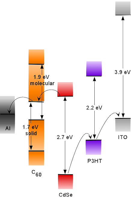
The photovoltaics we envision use quantum-confined, trap-free, crystalline semiconducting nanocrystals as both the light harvester and the artificial reaction center. Nanocrystals are an ideal light harvester. The band gap can be exquisitely tuned by controlling the size of the nanocrystal, thus the proper choice of size and type of nanocrystal allows one to create a photovoltaic with an absorption spectrum that matches the spectral distribution of sunlight. For example 20 angstrom CdSe has a band gap of 2.8 eV (450nm), 44 angstrom CdSe will harvest 600 nm light, and PbSe nanocrystals can harvest 1000 nm light. Thus the ideal efficiency of the photovoltaic is improved over a single thin semiconductor film, in which the energy of photons in excess of the band gap is wasted as heat. Quantum confinement in semiconducting nanocrystals leads to the emergence of a few discrete energy levels, thus the volume normalized oscillator strength is enhanced over the bulk material. High optical densities can, therefore, be achieved while maintaining the requirement of thin films. Perfectly crystalline CdSe nanocrystals are also an artificial reaction center, separating the electron hole pair on a femtosecond timescale. The nanocrystals have an intrinsic dipole moment originating from the top and bottom terminating planes of Se and Cd. Carriers are rapidly localized to the surface of the crystal where they remain for nanoseconds before recombining. The size-tunable band gap, large absorption coefficients, intrinsic electron hole pair separation, long exciton lifetime, and chemical robustness make nanocrystals the ideal material for photovoltaics.